- 您现在的位置:买卖IC网 > Sheet目录1222 > ISL21400USB-EVALZ (Intersil)EVAL BOARD FOR ISL21400
��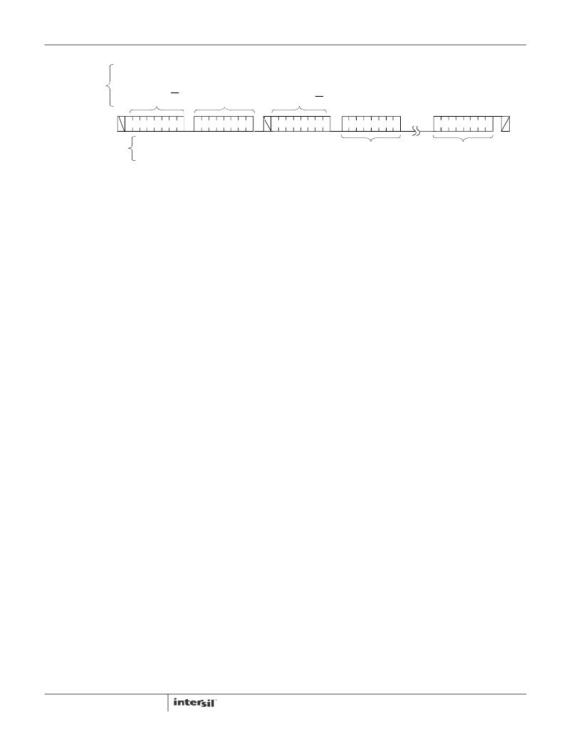 �
�
�ISL21400�
�IDENTIFICATION�
�SIGNALS�
�FROM� THE�
�MASTER�
�S�
�T�
�A� IDENTIFICATION�
�R� BYTE� WITH� R/W� =� 0�
�T�
�ADDRESS�
�BYTE�
�S�
�T�
�A�
�R�
�T� BYTE� WITH� R/W� =� 1�
�A�
�C�
�K�
�A�
�C�
�K�
�S�
�T�
�O�
�P�
�SIGNAL� AT� SDA�
�0� 1� 0� 1� A� A� A� 0�
�A�
�0� 0� 0� 0� 0�
�A�
�0� 1� 0� 1� A� A� A� 1�
�A�
�SIGNALS� FROM�
�THE� SLAVE�
�C�
�K�
�C�
�K�
�C�
�K�
�FIRST� READ�
�DATA� BYTE�
�LAST� READ�
�DATA� BYTE�
�FIGURE� 18.� RANDOM� ADDRESS� READ� SEQUENCE�
�Applications� Information�
�Power-Up� Considerations�
�DC� OUTPUT� CONTROL� DISCUSSION�
�The� reference� term� yields� Equation� 4� for� Reference� Output:�
�The� ISL21400� has� on-chip� EEPROM� memory� storage� for�
�the� DAC� and� gain� settings� of� the� device.� These� settings�
�V� OUT� (DC)� =� A� V� ?� V� REF� ?� A� REF�
�(EQ.� 4)�
�must� be� recalled� correctly� on� power-up� for� proper� operation.�
�Normally� there� are� no� issues� with� recall,� although� it� is� always�
�best� to� provide� a� smooth,� glitch-free� power-up� waveform� on�
�V� CC� .� Adding� a� small� 0.1μF� capacitor� at� the� device� V� CC� will�
�help� with� power-up� as� well� as� V� OUT� load� changes.�
�Noise� Performance�
�The� output� noise� voltage� in� a� 0.1Hz� to� 10Hz� bandwidth� is�
�typically� 90μV� P-P� .� The� noise� measurement� is� made� with� a�
�bandpass� filter� made� of� a� 1-pole� high-pass� filter� with� a�
�corner� frequency� at� 0.1Hz� and� a� 2-pole� low-pass� filter� with� a�
�corner� frequency� at� 12.6Hz� to� create� a� filter� with� a� 9.9Hz�
�bandwidth.� Load� capacitance� up� to� 5000pF� can� be� added�
�Note� that� the� DC� term� is� dependent� on� the� 1.20V� reference�
�voltage,� which� is� constant,� the� overall� gain,� A� V� ,� and� the�
�Reference� gain,� A� REF� .� Since� the� product� A� V� *A� REF� ranges�
�from� 0� to� 4,� the� total� reference� DC� output� can� range� from�
�0.0V� to� 4.8V.� In� order� to� get� the� 4.8V� output,� V� CC� must� be�
�greater� than� 4.8V� by� the� output� dropout� plus� any� overhead�
�for� output� loading� (the� specification� for� V� OUT� =� 5.0V� is� listed�
�with� V� CC� =� 5.5V).� The� Resolution� of� V� OUT� (DC)� control�
�changes� with� A� V� ,� so� that� with� a� 4.80V� full� scale� output�
�(A� V� =� 4),� the� resolution� is� 4.80/255� or� 18.8mV/bit.� With�
�A� V� =� 1,� the� resolution� is� 4.7mV/bit.�
�TEMP� SENSE� CONTROL� DISCUSSION�
�but� will� result� in� only� marginal� improvements� in� output� noise�
�and� transient� response.� The� output� stage� of� the� ISL21400� is�
�not� designed� to� drive� heavily� capacitive� loads.� For� high�
�impedance� loads,� an� R-C� network� can� be� added� to� filter� high�
�frequency� noise� and� preserve� DC� control.�
�Equation� 4� yields� this� expression,� Equation� 5,� for�
�Temperature� Slope:�
�V� OUT� (� TS� )� =� A� V� ?� V� TS� ?� A� TS�
�(EQ.� 5)�
�?� ?� ----------------------------------� ?� ?�
�V� OUT� =� ?� A� V� ?� V� REF� ?� ----------� ?� +� ?� A� V� ?� V�
�?� ?�
�?� ?�
�A� REF� =� ----------� (ranges� from� 0� to� 1)�
�A� TS� =� ?� ----------------------------------� ?�
�(� 2� ?� m� )� –� 255�
�?�
�?�
�255�
�Output� Voltage� Programming� Considerations�
�Setting� and� controlling� the� output� voltage� of� the� ISL21400�
�can� be� done� easily� by� breaking� down� the� components� into�
�temperature� variant� and� invariant,� and� setting� them�
�separately.� Let’s� use� Equation� 1� to� derive� separate�
�Reference� Output� and� Output� Temperature� Slope� equations:�
�?� n� ?� ?� (� 2� ?� m� )� –� 255� ?�
�255� TS� ?� 255� ?�
�=� {� A� V� ?� V� REF� ?� A� REF� }� +� {� A� V� ?� V� TS� ?� A� TS� }� ""�
�Reference� Term� +� Temp� Slope� Term�
�The� first� term� controls� the� output� DC� value,� and� the� second�
�term� controls� the� Temperature� slope,� where�
�n�
�255�
�(ranges� from� -1� to� +1)�
�14�
�Since� V� TS� =� K(T� -� T� 0� ),� the� slope� term� is� dependent� on� the�
�base� temp� slope� of� the� device,� K� (-2.1mV/°C),� and� the� gain�
�terms� A� V� and� A� TS� .� This� gives� a� formula� (Equation� 6)� for� the�
�portion� of� V� OUT� at� a� specific� temperature:�
�V� OUT� (� TS� )� =� A� V� ?� K� ?� A� TS� ?� (� T� –� T� 0� )� (EQ.� 6)�
�The� product� A� V� *A� TS� ranges� from� -4� to� 4,� so� the� Temperature�
�Slope� can� range� from� -8.4� to� +8.4mV/°C,� which� is�
�independent� of� the� output� DC� voltage.� The� resolution� of�
�Slope� control� is� determined� by� this� range� (±8.4mV/°C)� and�
�the� gain� terms,� and� will� vary� from� 65.8μV/°C/bit� (A� V� =� 4)�
�down� to� 16.2μV/°C/bit� (A� V� =� 1).�
�At� T� =� T� 0� =� +25°C,� V� OUT� (TS)� =� 0,� no� changes� in� A� TS� will�
�cause� a� change� in� V� OUT� ,� and� V� OUT� will� only� vary� with� the�
�V� OUT� (DC)� control.� As� temperature� increases� or� decreases,�
�from� T� =� +25°C,� V� OUT� will� then� change� according� to� the�
�programmed� Temp� Slope.�
�FN8091.3�
�March� 31,� 2011�
�发布紧急采购,3分钟左右您将得到回复。
相关PDF资料
ISL28210SOICEVAL1Z
EVAL BOARD FOR ISL28210 8SOIC
ISL28217SOICEVAL2Z
EVAL BAORD FOR ISL28217 8SOIC
ISL28218SOICEVAL1Z
EVAL BOARD FOR ISL28218 8SOIC
ISL28236SOICEVAL1Z
EVAL BOARD 1 FOR ISL28236 SOIC
ISL28248MSOPEVAL1Z
EVAL BOARD FOR ISL28248 MSOP
ISL28433TSSOPEVAL1Z
EVAL BOARD FOR ISL28433 14TSSOP
ISL54222IRUEVAL1Z
EVAL BOARD 1 FOR ISL54222IRU
ISL54406EVAL1Z
EVALUATION BOARD FOR ISL54406
相关代理商/技术参数
ISL21440
制造商:INTERSIL 制造商全称:Intersil Corporation 功能描述:Micropower Voltage Reference with Comparator
ISL21440_11
制造商:INTERSIL 制造商全称:Intersil Corporation 功能描述:Micropower Voltage Reference with Comparator
ISL21440IRTZ
功能描述:基准电压& 基准电流 ISL21440IRTZ MICRO PWR FGAFERENCE RoHS:否 制造商:STMicroelectronics 产品:Voltage References 拓扑结构:Shunt References 参考类型:Programmable 输出电压:1.24 V to 18 V 初始准确度:0.25 % 平均温度系数(典型值):100 PPM / C 串联 VREF - 输入电压(最大值): 串联 VREF - 输入电压(最小值): 分流电流(最大值):60 mA 最大工作温度:+ 125 C 封装 / 箱体:SOT-23-3L 封装:Reel
ISL21440IRTZ-T13
功能描述:基准电压& 基准电流 ISL21440IRTZ MICRO PWR FGAFERENCE RoHS:否 制造商:STMicroelectronics 产品:Voltage References 拓扑结构:Shunt References 参考类型:Programmable 输出电压:1.24 V to 18 V 初始准确度:0.25 % 平均温度系数(典型值):100 PPM / C 串联 VREF - 输入电压(最大值): 串联 VREF - 输入电压(最小值): 分流电流(最大值):60 mA 最大工作温度:+ 125 C 封装 / 箱体:SOT-23-3L 封装:Reel
ISL21440IUZ
功能描述:基准电压& 基准电流 ISL21440IUZ MICRO PWR FGAFERENCE RoHS:否 制造商:STMicroelectronics 产品:Voltage References 拓扑结构:Shunt References 参考类型:Programmable 输出电压:1.24 V to 18 V 初始准确度:0.25 % 平均温度系数(典型值):100 PPM / C 串联 VREF - 输入电压(最大值): 串联 VREF - 输入电压(最小值): 分流电流(最大值):60 mA 最大工作温度:+ 125 C 封装 / 箱体:SOT-23-3L 封装:Reel
ISL21440IUZ-T13
功能描述:基准电压& 基准电流 ISL21440IUZ MICRO PWR FGAFERENCE RoHS:否 制造商:STMicroelectronics 产品:Voltage References 拓扑结构:Shunt References 参考类型:Programmable 输出电压:1.24 V to 18 V 初始准确度:0.25 % 平均温度系数(典型值):100 PPM / C 串联 VREF - 输入电压(最大值): 串联 VREF - 输入电压(最小值): 分流电流(最大值):60 mA 最大工作温度:+ 125 C 封装 / 箱体:SOT-23-3L 封装:Reel
ISL22102
制造商:INTERSIL 制造商全称:Intersil Corporation 功能描述:32 Tap, Push-button, Dual Audio Logarithmic Potentiometer with Buffer Amplifiers and Audio Detection
ISL22102IR20Z
功能描述:数字电位计 IC 32 TAP PUSH-BUTTON DL AUD LOG W/BUFR RoHS:否 制造商:Maxim Integrated 电阻:200 Ohms 温度系数:35 PPM / C 容差:25 % POT 数量:Dual 每 POT 分接头:256 弧刷存储器:Volatile 缓冲刷: 数字接口:Serial (3-Wire, SPI) 描述/功能:Dual Volatile Low Voltage Linear Taper Digital Potentiometer 工作电源电压:1.7 V to 5.5 V 电源电流:27 uA 最大工作温度:+ 125 C 安装风格:SMD/SMT 封装 / 箱体:TQFN-16 封装:Reel